CH-02 IGCT (Integrated Gate Commutated Thyristor)
The Integrated Gate-Commutated Thyristor: A New High Efficiency, High Power Switch for Series or Snubber less Operation
Abstract
A novel high power semiconductor switch is now commercially available. The IGCT combines in a unique manner the advantages of a thyristor, low on-state voltage drops and high blocking voltage ratings, with the rugged switching behavior of the transistor. After a brief overview of the technology used, the main characteristics of the 5SHY 35L4502 are presented. Finally, examples for possible applications are given.
1. Introduction
Development of GTO technology has led to a wide variety of applications in the range of 1 to 20 MVA, mainly adjustable speed drives and railway interties. Although these applications have proven the reliability and cost effectiveness of the GTO thyristor, there are still cumbersome disadvantages of this technology. The inhomogeneous switching mode of the GTO gives rise to the need for dv/dt limiting snubber capacitors, and large dispersions in turn-off times complicate the series connection of GTOs.
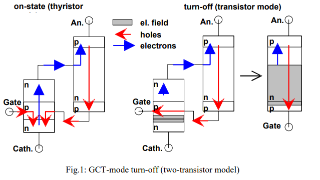
Recently a breakthrough in GTO technology was achieved by the introduction of the “Hard Driven GTO” leading to the possibility of snubber less switching [1]. This novel switching mode is characterized by an extremely fast commutation of the cathode current to the gate (Gate Commutated Thyristor) whereby the cathode emitter is turned off before the voltage at the main blocking junction rises (see Fig. 1). To achieve this the whole cathode current is commutated to the gate within less than 1 µs. Any regenerative action from the cathode which might lead to filamentation is therefore prevented, leaving just the p-base – n-base – anode emitter – pnp transistor active during turn-off. This turn-off mode led to the name of the new device: As well known from the IGBT, a transistor turn-off mode is very favorable for high turn-off ratings without a snubber.
As mentioned above, a GCT is able to turn off high currents even without a snubber. Fig. 2 shows a GCT turning off 3 kA at a dc-voltage of 2.5 kV (VDM = 4.5 kV) without any dv/dt limitation. Typical of the technology used, is a high tail current but short tail phase (see below). The height of the tail current is governed by the amount of free charge carriers present in the device. In this case, the device is optimized for low on-state losses, the amount of carriers is high and so too is the tail current.
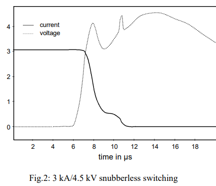
The voltage peaks in Fig. 2 are caused by the current slopes during turn-off and during the cut-off of the tail current in combination with the unclamped stray inductance of the circuit of about 500 nH.
Another important advantage, inherent in the GCT turn-off mode, is a strong reduction in turn-off time. Due to the high gate currents during commutation, the storage time is drastically reduced to only 3 µs including triggering delay of the gate driver. As the total variation of the turn-off time reduces to only 300 ns, series connection of GCTs is easily realized.
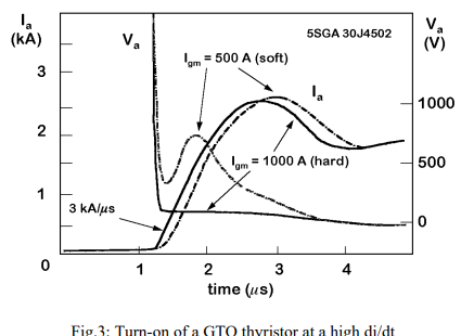
The same principle can be used to radically improve the turn-on behavior of the GCT. As seen in Fig. 3 GTOs usually need some time for the on-state voltage to fall to the stationary value. This is because the carriers injected from the anode need a few microseconds to reach the cathode. This can be ameliorated by using a sufficiently high rise of the gate current allowing the cathode – p-base – n-base transistor to carry the whole anode current without a major voltage drop. Again, this transistor action represents a homogenous turn-on, which cannot lead to an inhomogeneous current distribution. Additionally, the turn-on losses are drastically reduced [4]. Generally, it can be stated that GCT switching is realized by forcing the thyristor into a transistor mode. This leads to a unique combination of the advantages of the thyristor with those of the transistor. Because the inductance of the standard packaging technology of GTOs, in combination with a long coaxial cable to the gate driver, would need a bulky and costly gate driver to the achieve the high (di)gate/dt, the concept of an integrated gate driver was developed: A novel low inductance GCT package is contacted directly to the GCT gate driver, giving an overall gate inductance of less about 4 nH. Gate turn-off pulses with more than 4 kA/µs can now be realized with a driving voltage lower than 20 V. This, in turn, allows the use of a single voltage source for turn-off and
for blocking.
2. Buffer Layer Transparent Emitter Technology:
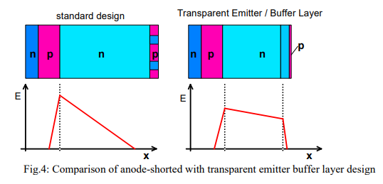
Field experiences and long-term blocking tests have shown in the past few years that cosmic radiation impact in combination with high electric field strengths can lead to instantaneous destruction of GTOs. For the standard GTO design, the resulting need for lower electric fields leads to thicker devices which, in turn, leads to higher on-state and switching losses. The GCTs are now consequently designed with a new technology, the buffer layer transparent emitter design, which gives a much better trade-off between the capability to withstand cosmic radiation and the silicon thickness [2,3]. The Transparent Emitter technology uses a very thin anode emitter which allows part of the electrons to recombine at the contact metal interface – without generating holes. The emitter efficiency is, therefore, reduced without shorting the anode. The introduction of an n-buffer layer is now possible. As shown in Fig. 4 a trapezoidal distribution of the electric field can now be realized, which leads to a lower maximum field strength at even higher blocking voltages. Compared to a conventional GTO design, silicon thickness can be cut by 1/3 giving even a higher capability to withstand cosmic radiation and cutting total losses to a minimum.
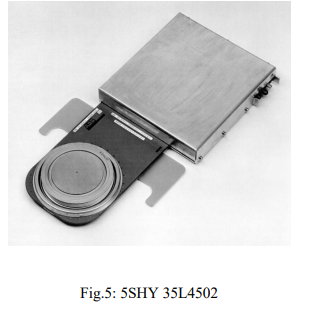
A first device is now commercially available from ABB Semiconductors which includes all the features mentioned above:
- 91 mm diameter GCT wafer with transparent emitter technology.
- cosmic radiation withstand capability 100 fit (failures in time) at 2.8 kV dc.
- turn-off rating (non.rep.) up to 5 kA at Cs = 4µF and VDM = 4.5 kV
- low on-state, type 2.8 V at 5 kA (125°C)
- 5″ low inductance housing integrated in gate driver needing only voltage and current supply
- optical trigger input
- optical status monitor
3.Chacteristics:
On-state
The standard device is optimized for a low to medium frequency high power applications. The goal was to develop a device suitable for series connection, which is inherent in the GCT, realizing an extremely low on-state by a consequent implementation of the transparent emitter technology while achieving high turn-off capability, which, again, is inherent in the GCT. Fig.6 presents a chart of the onstate characteristics showing minimum, typical and maximum values of the on-state voltage up to 5 kA at 125°C.
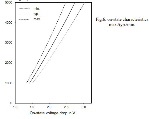
These characteristics allow an RMS current rating of up to 2200 A (Half sine wave, 50 Hz) at Tcase = 85°C.
Turn off
Due to the homogenous switching mode, the turn-off capability is greatly increased. That is the reason why even GCTs optimized for low on-state and low turn-on losses still exhibit high turn-off capability. The turn-off ratings of the 5SHY 35L4502 and the typical values for the corresponding turn-off losses are summarized in Table 1 (non-repetitive values):

Fig. 7 shows a GCT turn-off at 5 kA with a snubber capacitor of 4 µF. Snubber inductance is > 200 nH. Again, a high tail-current short tail-phase, typical for buffer layer design, is evident. This tail-current can be reduced by different irradiation techniques generating lower turn-off losses but slightly higher on-state voltages.
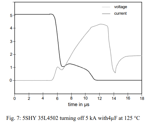
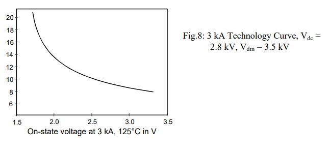
Fig 8. depicts a trade-off curve for the buffer layer technology at CS = 0 µF and different electron irradiation levels. It shows, that for a current level of 70 A/cm2 the turn-off losses can be reduced
by a factor of 2 taking by allowing an increase of on-state voltage to only 3.0 V. The 5SGY 35L4502 can, therefore, cover a wide range from low on-state/low frequency to higher on state/higher frequency industrial or traction drive applications.
Application Example:
Series connection:
Compared to the standard GTO one of the IGCT’s most prominent benefits is the short storage time which is accompanied by very small tolerances in total turn-off time. The device is, therefore, very well suited for high power applications, where series connection of elements is required.
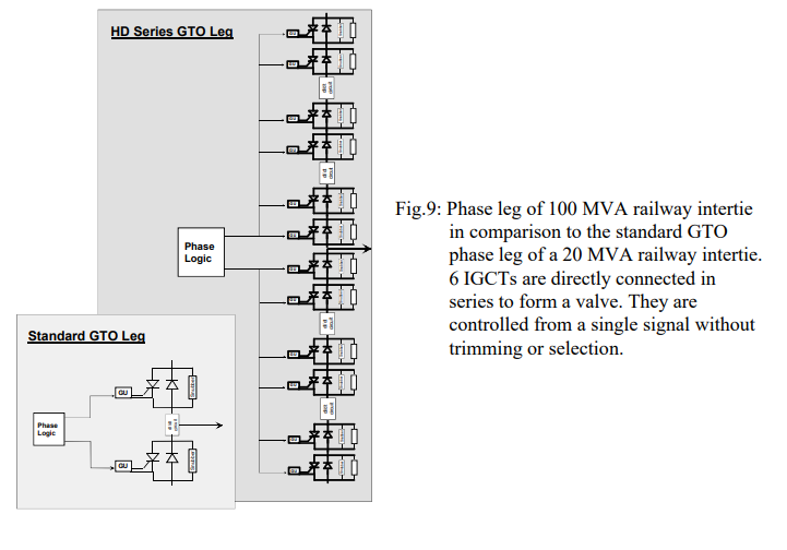
Fig.9 shows the topology of the output stage connected to the railway network: it contains 24 phase-leg modules operating from a nominal 10 kV DC-link with rated phase output current Irms = 1430 A. In every phase leg, 12 devices operate in two blocks of 6 directly series-connected IGCTs. No selection or trimming is required to obtain £ ±10% tolerance of the IGCTs’ peak turn-off voltage under series connection, and thus a redundancy of 2 elements per switching position was achieved. A first 100 MW railway intertie based on IGCTs commissioned in 1996 has now been operating 9 months without any failures of IGCTs or their power supplies. With a total of 288 actively switching IGCTs, more than 1.8 million device-operating-hours have been accumulated, clearly demonstrating the reliability of the IGCT concept.
Traction converters
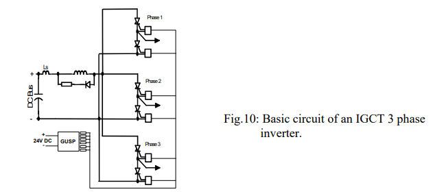
A family of reverse conducting IGCTs for drive applications is currently being developed. Due to the possibility of snubber less switching, IGCT-based converter systems can be much more compact than GTO-based systems. Fig. 10 shows a possible circuit for a 3-phase inverter: Only one di/dt limiter is required per inverter, and gate-drive power-supply is centralized, to further reduce inverter volume.
Two types of clean water cooled 3(-4) phase inverters have been studied in detail so far. Both incorporate IGCTs, a di/dt limiter, isolated gate-drive supply, water-distribution and the mechanics required and operate from a nominal 2.8 kV DC-link. The following features have been obtained in the study:


Although still not completely optimized, this is believed to represent the highest power densities in the industry for this class of converter. More details will be published at a later date.