CH-04 ACS5000W Power Hardware Gen-01
Objective:
Upon completion of this module, you will be familiar with the generation 1 of the water-cooled ACS 5000 hardware configuration and you will be able to describe and explain to others the main circuit diagram. In addition, you will be able to describe the function and location of the power and control hardware components as well as the implemented protection functions.
Overview:
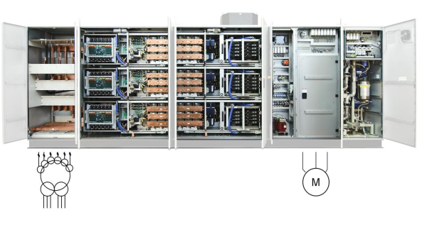
The water-cooled ACS 5000 is a voltage source frequency converter of the ACS product family. The water-cooled version extends the 2 to 7 MVA power range of the air-cooled ACS 5000 series to the 5 to 24 MVA power range. The drive is available for standard motors with voltages up to 6.9 kV. The drive features several proven ABB technologies including Multilevel-Fuse less Voltage Source Inverter design, Direct torque motor control platform, and IGCT power semiconductors. The water-cooled ACS 5000 features a modular design based on standardized cabinet units. Each unit is dedicated to a specific function. The main units are the Terminal Unit for the transformer cables, the Line Supply Unit, the Inverter Unit, the Control Unit together with the Terminal Unit for the motor cables and the Water-Cooling Unit.
Main Circuit Diagram (Single INU):
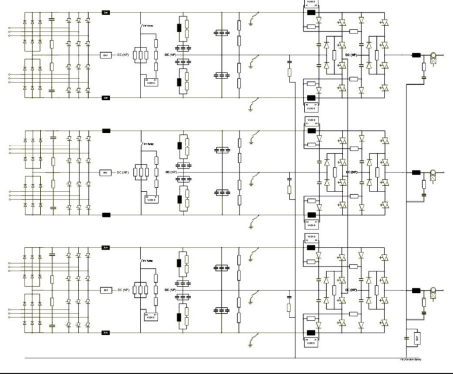
Here is the main circuit diagram of a single Inverter Unit configuration. As you can see, three identical phases are used to drive the motor. According to the function, the power hardware consists of the following parts: Diode rectifier bridge, snubber circuit, thyristor crowbar, di/dt choke, diode failure supervision, discharging circuit, soft-coupled DC link, hard coupled DC link, balancing resistors, DC link grounding switch, Neutral Point to ground filter, Inverter, EMC filter, common mode filter with earth fault supervision, and output current measurement.
Parallel Inverter Unit:
The parallel Inverter Unit topology is used for applications requiring a motor current greater than 1000
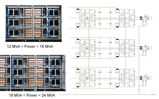
A. The second Inverter Unit is located to the right of the first Inverter Unit and the outputs of both INU’s are connected to the same motor. The motor can either have a single or a double winding system. For applications requiring more than 12 MVA but less than 18 MVA output power, two Inverters will be used in parallel. In case the power needs to be bigger than 18 MVA, an additional capacitor bank needs to be installed next to the two INU’s.
Line Supply Unit (LSU):
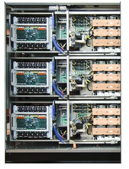
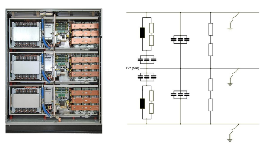
The Line Supply Unit LSU rectifies the AC line voltage and supplies electrical energy to the DC link capacitors. Three identical diode rectifier power cells are combined to a network-friendly 36-pulse system which is supplied by one or two input transformers with a total of six isolated secondary winding systems. Two different water-cooled LSUs with different electrical ratings and semiconductors are used in the water-cooled ACS 5000: The 12 MVA version for single inverter configurations, and the 24 MVA version for parallel inverter configurations. The main components in the LSU are: The diode rectifier phase modules, the EAF board for diode failure supervision, the grounding switch, the discharging circuit, and the soft coupled capacitors. The protection firing choke, and the balancing resistors are behind the EAF and the discharging circuit.
Diode Rectifier Phase Module:
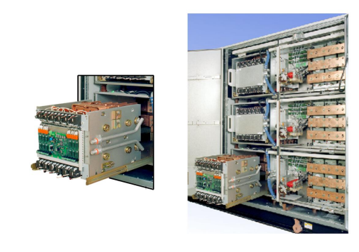
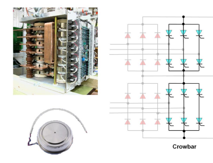
The rectifier phase modules are mounted on sliding rails and can be extracted from the power cell for maintenance and service tasks. Each module includes: 12 rectifier diodes, 12 crowbar thyristors and 12 pulse transformers. The Pulse transformer Interface board PINT is also located on the diode rectifier phase module. The total weight is approximately 200 kg, so please take care when taking out the module to perform any work.
Rectifier:
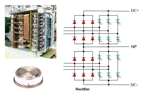
Three 12-pulse diode bridges are used as input rectifier to supply DC voltage and current to the DC link. The full DC bus current flows through the upper and lower diode bridge and the DC voltages are added up. With this arrangement of the diodes, the ACS 5000 gets three DC link potentials: DC plus, Neutral Point and DC minus. Another benefit of this arrangement is the lower harmonics.
Thyristor Crowbar:
The thyristor crowbar is a protection circuit which is activated should a short circuit occur in the drive. The thyristors are used for protection purposes only and don’t participate in the rectification. In case a short circuit is detected somewhere in the drive, the “Firing Through” function will generate a full ON-state of all crowbar thyristors in the LSU’s and all IGCT’s in the Inverter Units. The high short circuit currents will be shared by all semiconductors so that the stress on the fault is reduced. By applying protection firing, the rectifier is shorted to prevent further damage of the converter. The crowbar circuit consists of 12 thyristors per phase. The firing pulses are sent to the thyristors from the Pulse transformer Interface board via pulse transformers.
Snubber Circuit:
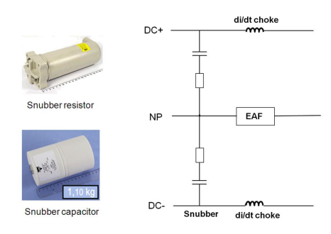
In order to prevent harmful overvoltage when diodes turn off the three rectification phases are snubbed by two RC snubbers, one installed between DC plus and the Neutral Point and the other between the Neutral Point and DC minus. The snubber circuit is limiting the rate of the voltage rise across the diodes and the crowbar thyristors. The transient current peaks due to the semiconductor switching is limited by two DC chokes. When protection firing happens, those two chokes will also limit the current through the thyristor crowbar.
Balancing Resistor:
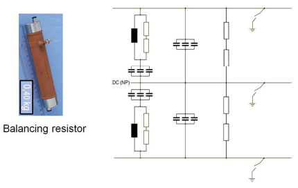
The balancing resistors are connected between the DC link bus bars. They are used to clear static unbalances in the DC link. Furthermore, these resistors guarantee discharging of the system even without auxiliary power.
DC Link Grounding Switch:
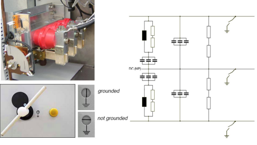
The drive is equipped with three grounding switches. The switches are safety devices ensuring personnel a save access to the drive once it is grounded. Grounding the drive is also a precondition to open the doors of the medium voltage sections. The grounding switches are operated using a removable lever. The lever is attached at the inside of the control section door. Operation of the grounding switches is released by the drive. The release is indicated by the lamp GROUNDING SWITCH UNLOCKED. The lamp lights up when the main power supply for the drive has been switched off and the capacitors of the DC links have been discharged. The window next to the opening for the grounding switch lever indicates the grounding switch position. When a switch is in position grounded, the plus, minus and neutral point of the associated power cell is connected to protective earth.
DC Link Capacitor:
In the Line Supply Unit, the capacitors are soft coupled to the DC bus through a series connection of a reactor in parallel with a damping resistor. The water-cooled DC link capacitors smooth the DC voltage and decouple the rectifier from the inverter. The reactor limits the current rise in the event of crowbar firing. During protection firing, the soft coupled capacitors are not participating in the beginning, which will lower the current peak compared to the hard coupled DC link. But this configuration will also make it more difficult for the DC voltage control, so the hard coupled DC link is also necessary. The hard coupled DC link capacitors are located in the Inverter Unit. Unlike the capacitors in the LSU, the capacitors in the INU are directly connected to the DC bus. The water-cooled capacitors have the same function as the soft-coupled capacitors in the LSU: smoothing the DC voltage and decoupling the line rectifier from the inverter.
LSU Control Overview:
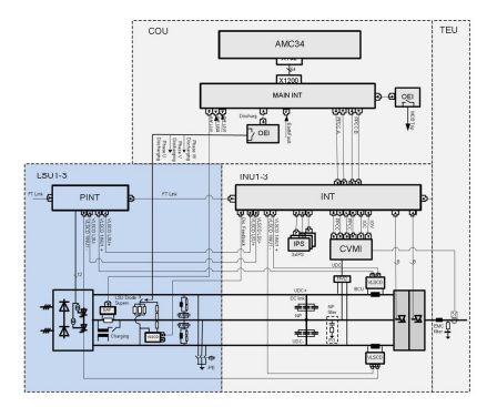
In ACS 5000, the main control board is AMC in the Control Unit. The AMC board not only controls the supervision and protection of both the rectifier and the inverter, but also the MCB and the Water-Cooling Unit. The main Interface board is used to build up the communication between the AMC and the three phase module Interface boards. It communicates with the AMC board via a 64-pin ribbon cable. Each phase module has a local Interface board, which contains the local modulator, fast protection functions and measurement interfaces. Because the LSU is a diode rectifier, it does not need any control. But three control boards are used for protection and supervision of the LSU. The PINT board is used to control the crowbar thyristors in case of a protection firing. The EAF board is used to supervise the rectifier diodes. And the VLSCD board is used to supervise the discharging function.
PINT Board:
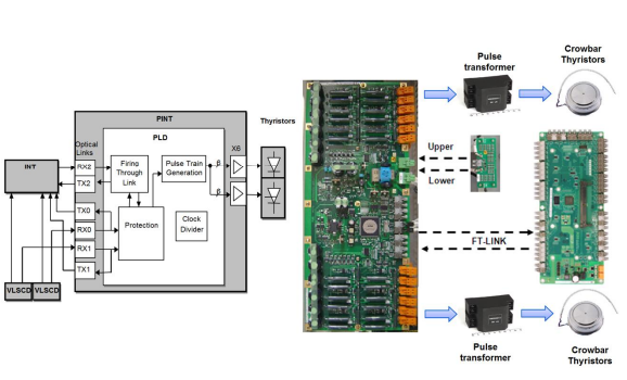
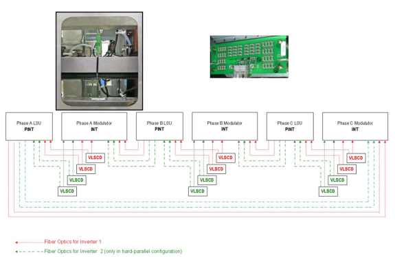
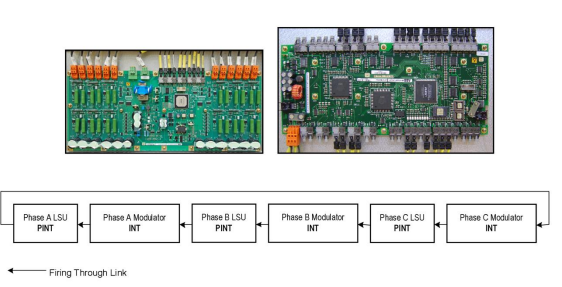
The Pulse transformer Interface board PINT is located on the diode rectifier phase module. It can switch on the crowbar unit to protect the line side in case of a short circuit. Each PINT board controls 12 independent crowbar thyristors with electrical amplifiers. The logic on the PINT board handles the serial protocol via the optical links and generates pulse trains for all thyristors. The crowbar in LSU can be activated either by the Firing Through link or by the short circuit signal which is generated by the VLSCD boards in INU. The Firing Through link is a ring topology of unidirectional serial fiber optic point-to-point connections. The connection between all phase INT and all PINT boards will establish a fast and safe connection to start the crowbar firing. The PINT boards are also supervising the short circuit signals from the VLSCD’s. Pulse transformers are used between the control electronics and the crowbar thyristors for galvanic isolation.
Rectifier Diode Failure Supervision:
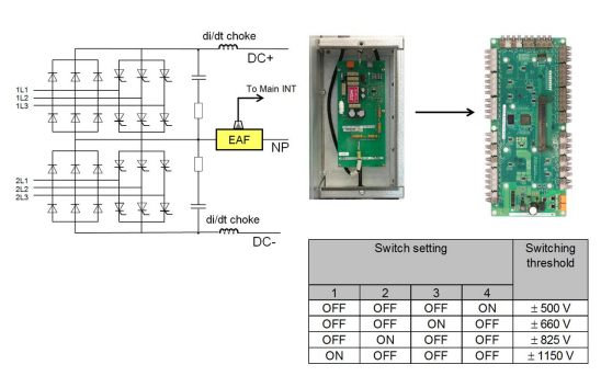
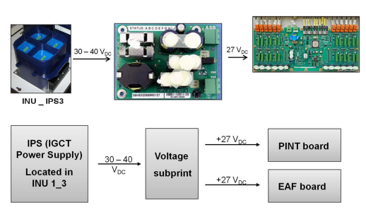
The LSU diodes are supervised by an EAF board, which is measuring the voltage between the Neutral Point of the 12-pulse bridge and the Neutral Point of the INU. Normally, the voltage between these two points is small. But in case of a broken component in the rectifier, the voltage measured by the EAF board will exceed the threshold value and an optical fault signal is sent to the main Interface board. The threshold value is set by DIP switches on the EAF board. The default setting is 825 V. The EAF board is supplied by 27 VDC from the third IPS in INU via the voltage sub-print.
Single Voltage Sub-Prints:
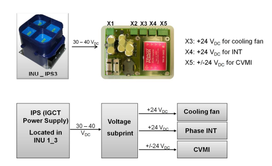
To supply the control boards in the LSU, a single voltage sub-print is used to convert the unregulated 30 to 40 VDC output from IPS3 in INU to a regulated output voltage. Two +27 VDC outputs are used for the PINT and EAF boards. Two LED’s are used to indicate if the sub-print is working properly.
Discharging Circuit:
In the water-cooled ACS 5000 there are three physical discharging circuits. All three DC links will be discharged at the same time. The discharging sequence is started with a fiber optic signal from the Main INT board in COU. The OEI board converts this optical command to an electrical signal which controls the three parallel high voltage discharging relays at the same time. Because of that it is not possible to discharge each DC link separately. There is a parameter named “Discharge level” in the application software. Drive is considered as discharged only after the measured DC voltage level in each DC link is below the level defined by this parameter. Only after drive is discharged, it can be grounded, and the cabinet door locking is released. The feedback signals from the VLSCD boards supervising the discharging hardware are routed to the Phase INT board. It should be active only during discharging. Otherwise, the high voltage relay is probably broken, that means it stays closed. Discharging without the Water-Cooling Unit running would cause overheating of the discharging resistors. Therefore, discharging is not allowed if the water cooling is not running. Instead, the balancing resistors will be used for discharging.

Inverter Unit 1 (INU-01):
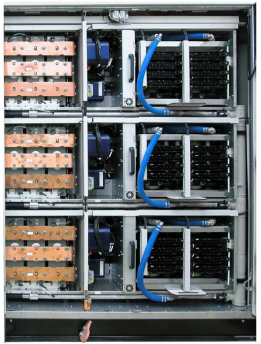
The Inverter Unit INU converts the DC voltage to the required AC motor voltage. With three identical\ IGCT phase modules, the Inverter Unit is designed as a self-commutated, 5-level Voltage Source Inverter which allows four-quadrant operation. One INU can deliver an output current of up 1000 A. The main components in the INU are the hard coupled DC link capacitors, the IGCT power supply units, the Phase INT and the Current and Voltage Measurement Interface boards and the inverter phase modules.
Inverter Unit 2 (INU-02):
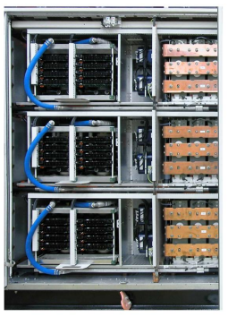
INU2 will be used in parallel with INU1 if higher power is needed. There are no control boards in this unit. The IGCT modulation control is done by the INT board in INU1.
Air to Air Heat Exchanger:
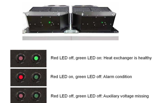
All water-cooled drives are additionally equipped with a roof-mounted air-to-air exchanger on each INU. The heat exchanger ensures a constant air flow through the cabinet section thus transferring the heat from non-water-cooled components to the exterior. The Inverter Unit can optionally be equipped with two air-to-air heat exchangers if redundancy or extended cooling is required. The fans of the heat exchanger are controlled via a digital output of the drive control system. The fans are switched on together with the main circuit breaker. Two LED’s on the heat exchanger inform about the status of the unit. Alarm signals are also shown on the CDP control panel.
Inverter Phase Module:
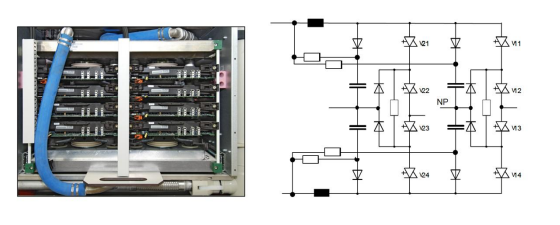
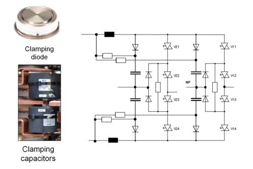
Two three level power cells are used in parallel on each phase module: one for motor supply and the other one for the common rail connection. The extractable inverter phase modules facilitate maintenance and service on the unit. Each phase module contains: 8 Reverse Conducting IGCT’s, 4 Neutral Point diodes, 4 clamping diodes, 4 clamping capacitors and two balancing resistors. The four clamping resistors are installed on the drive frame.
Integrated Gate Commutated Thyristor:
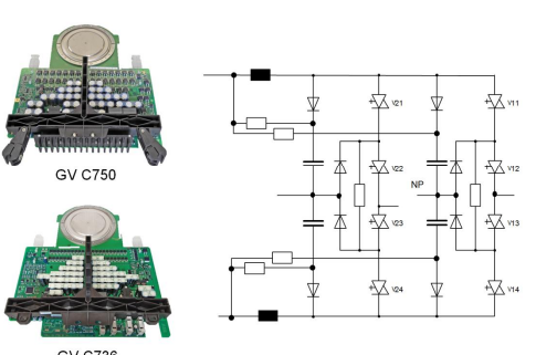
RC-IGCT’s are used as switching devices in the inverter. That means, that the freewheeling diode, also called Reverse Conducting diode, is integrated in the semiconductor package. Two types of RC-IGCT’s are used in the water-cooled ACS 5000. The old type is using the Gate Driver type GV C750 and the new IGCT is using the Gate Driver type GV C736..
Neutral Point Diodes (NP Diodes):
The Neutral Point diodes divide the DC voltage equally across the IGCT’s and protect the components when the IGCT’s of the other leg are turned off. More importantly, they connect to the NP potential to form a 3-level inverter bridge which increases the freedom of the output vector control and improves the quality of the output waveform.
Balancing Resistor:
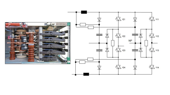
Balancing resistors provide voltage sharing when all IGCT’s are turned off and prevent unbalance between half DC link voltages.
Clamping Circuit:
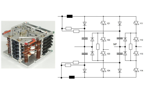
The clamping circuit formed by diodes, resistors and capacitors will discharge the energy stored in the di/dt chokes, inverter diodes and IGCTs. It protects the components against excessive voltages formed over the chokes when an IGCT is turned off.
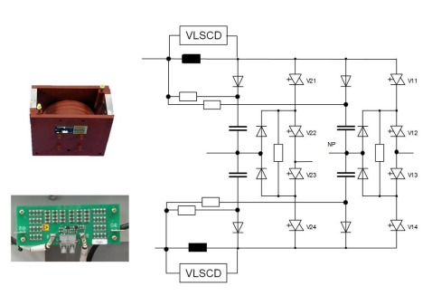
di/dt chokes:
Two chokes are used to limit the current rate of rise in the negative and positive DC bus. They are needed to protect diodes and IGCT’s from excessive di/dt. In case of short circuit or firing through the di/dt chokes will also limit the current and current rate of rise. In each INU there are two VLSCD boards. The boards are installed in parallel with the di/dt chokes on the DC bus. They are used to monitor the inverter for short circuits.
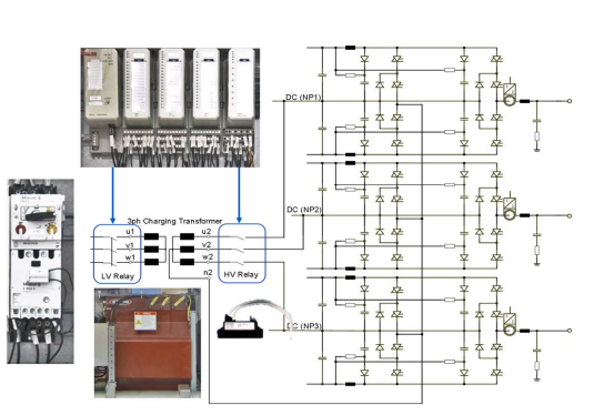
Charging Circuit:
A three-phase step up transformer is used to pre-charge the capacitors of all three DC links at the same time. The secondary windings of the charging transformer are connected to the Neutral Point of each phase and the star point of the transformer is connected to the common rail. Through digital outputs of a S800 module, the control system can switch on the input low voltage relay and the output medium voltage relays. The reverse conducting diodes of the IGCT’s in the inverter act as charging rectifier.
Charging Sequence:
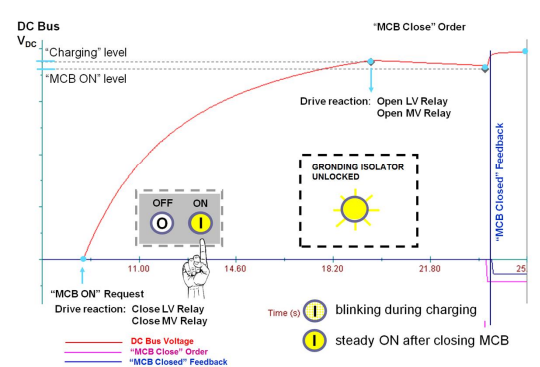
The charging sequence, including the MCB close command, is automatically controlled by the drive. If the drive is in Ready On state, meaning no faults pending and all 3 grounding switches are open, an external “MCB ON” request will initiate the charging sequence. “MCB ON” request is the only external command needed and can be given either by pressing the “ON “button on the door in “Local” mode, or by the overriding system in “Remote”. Once the charging sequence is initiated, the grounding switches will be locked and the lamp “GROUNDING ISOLATOR UNLOCKED” will go OFF.
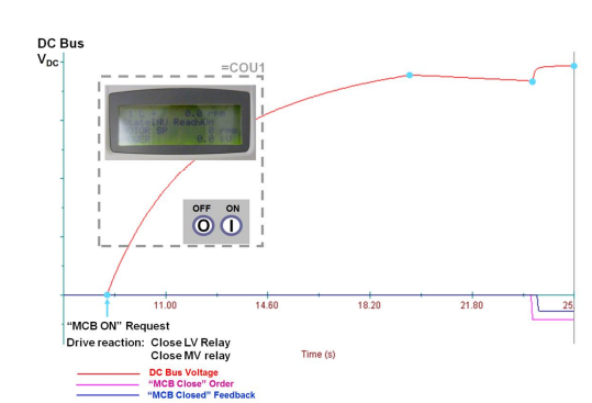
During the charging sequence, from the moment “MCB ON” request was given until MCB is actually closed, the “ON” lamp is blinking. After the drive started charging, the lamp “GROUNDING SWITCH UNLOCKED” on the door will go OFF and the grounding switches will be locked. After MCB is closed, the “ON” lamp will be steady ON. Once “MCB ON” request is given, the drive control will perform the following actions: It will close both LV Relay and MV Relay. The charging circuit will be energized, and the DC link capacitors will start to charge. The “ON” lamp flashes. When DC bus voltage reaches the “Charging” level, the control will open both relays, and the actual DC link voltage level is memorized. The capacitors will start to discharge via the balancing resistors. Then the LV side charging relay will be closed for a short time and at the same time the actual DC link voltage is compared to the previously memorized DC voltage level. If the actual DC voltage starts to increase again while only the LV side relay is closed, the MV side charging relay is considered to be broken. If the relay test was successful and when the DC voltage reaches the “MCB ON Level”, the control gives the MCB close order. The MCB is closed, and the DC bus voltage jumps to the maximum value. The “ON” lamp will turn steady on.
INU Control Overview:
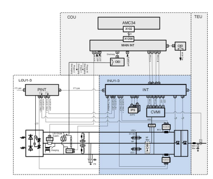
In the Inverter Unit, the Interface board INT generates the firing pulses for the IGCT’s according to the commands from the AMC board. Furthermore, the INT board centralizes all measurements and includes fast software protection functions. The Current and Voltage Measurement Interface CVMI converts DC voltage and phase current measurements to numeric values. The CVMI also includes hardware-based overcurrent detection. The High Voltage Divider board measures the DC voltages and transfers the results to CVMI. Two Voltage Level Short Circuit Detection boards allow the interface board to detect IGCT faults and short circuits. Three IGCT Power Supply units feed auxiliary power to all IGCT’s and some printed circuit boards via voltage sub-print.
Control Boards in INU:
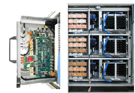
The phase INT and CVMI boards are located in the INU and are installed in a drawer. The phase Interface board serves as a communication interface to the control system in the COU. The pulse firing logic for the IGCT’s and the fast protection functions are integrated on the board as well. The CVMI board serves as a current and voltage measurement interface. The actual current value from the current transducer and the actual DC voltage values from HVD are converted to fiber optic signals which are sent to the Interface board. A small voltage sub-print here is used to supply the power for those two boards.
Phase Interface board:
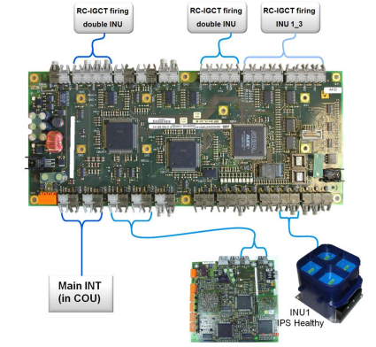
The software to control the modulation, the fast protection functions and the PPCS communication is stored on two EPLD’s. The EPLD software version must be compatible with the type of the unit and with the software versions in other control boards in ACS 5000. The software of the EPLD’s can be downloaded to the INT board using the appropriate Altera or Xilinx programming tool. The software can be found on the ABB MV Drives Portal. Fiber optic cables are used for transmission of data between the Interface board and other printed circuit boards. The grey colored fiber optic connectors are used to transmit light signals to other boards and the black colored connectors receive light signals from other boards. A pair of one transmitter and one receiver form a fiber optic channel.
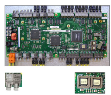
2 PPCS communication channels are used between the phase INT and the main INT board in Control Unit. They are called Link A and Link B. 2 other PPCS communication channels are used between CVMI and INT. Those are Link C and Link D. In addition, a low active light signal is connected from CVMI to phase INT board to indicate a hardware overcurrent. The INT board is also generating the switching commands for the 8 IGCT’s in a single INU configuration or the 16 IGCT’s in case of a double INU configuration. Furthermore, the INT board is supervising the IPS units which deliver the control power to the gate drivers of the IGCT’s. Each IPS sends a low active optic signal to the INT. Water cooled ACS 5000 has three physical discharging circuits. To indicate if the discharging function is working properly or not, a feedback signal from the VLSCD board routed to PHASE INT. They should come only during discharging. Otherwise, HV relay is assumed to be broken.
Shrot Circuit Detection :
Two VLSCD boards per INU are used to detect short circuits and IGCT malfunction. They are connected in parallel with the di/dt chokes. To enhance safety, the short circuit detection is redundant. Each VLSCD board has two transmitters: one to the Interface board of the same INU and one to PINT board in LSU of the same phase. The PINT in LSU sends the signal further to the INT board of the next unit. This way, two INT boards can detect a short circuit situation. Each board monitors the voltage across the choke and sends a light pulse of a fixed duration through a fiber optic cable to the control boards mentioned above. A current rise in the choke due to a short circuit lead to a voltage rise which in turn increases the pulse duration of the monitored signal. If the pulse duration remains more than a certain allowable time, a short circuit has occurred. The protection firing is initiated immediately to protect the drive from further damage.
FT Link or Firing Through Link:
The FT link is a ring connection through all phase INT and PINT boards. In case of a serious fault which requires a Firing Through protection reaction, each INT board will turn all IGCT’s, and each PINT board will turn on all crowbar thyristors simultaneously to avoid further damage in the drive.
INT2 Board:
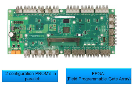
A new version of the Interface board called INT-2 replaced the INT board in ACS 5000 in 2011. The interface connections are the same as with the old INT board. It is based on the FPGA technology. It is equipped with programmable memories and has better link handling, better EMC design and improved ACS 5000 diagnostics implemented. This board supports a serial and a parallel interface to the AMC board, so it can be also used as the main interface board, directly connected to the AMC-34 board via a 64-way ribbon cable. The software of the EPLD’s can be downloaded to the INT-2 board using the appropriate Xilinx programming tool. The software can be found on the ABB MV Drives Portal .
Current and Voltage Measurements (CVMI) Boards:
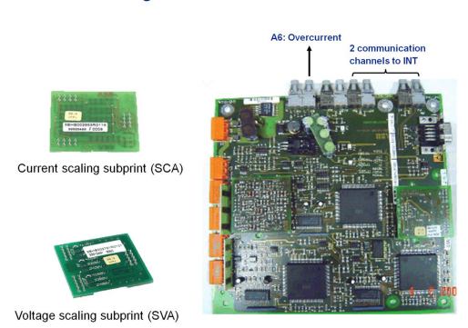
The CVMI board is the measurement interface board. The actual DC voltage and AC current signals are measured here. The measurement results are converted into an optical signal and transferred to the phase INT board through two PPCS channels. In addition, one optical output A6 is connected to the INT board for the status of overcurrent detection. This is a low active signal. The overcurrent detection compares the analogue value of the current input with a predefined threshold value. If overcurrent is detected, the light on the fiber optic output will be switched off. The measurement scaling of current and voltage is done by two removable scaling sub-prints. There is a Current Scaling sub-print and a Voltage Scaling sub-print. Different types of SCA boards are used for different current measurement ranges. It is important, that the sub-print matches the power rate of the converter. This should be checked before starting the commissioning. Otherwise, the current measurement is wrong which could damage the drive or other system components.
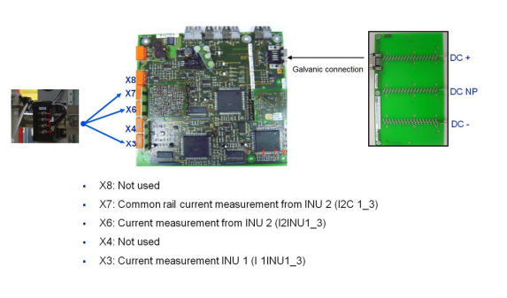
The HVD board takes care of the voltage division from high voltage down to the low voltage input range of the CVMI. This board is equipped with passive components only and does not require a supply voltage. The current measurement device is a current transducer. The actual phase current signal is connected to the CVMI board on terminal X3. In case of a double INU configuration, the second actual phase current signal from INU2 will be connected to the CVMI board on terminal X6. Additionally, X7 will be used for the common rail current measurement of INU2.
IGCT Power Supply:
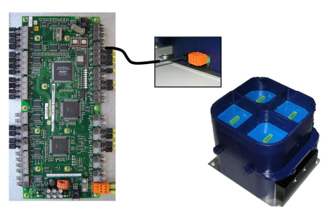
The IGCT Power Supplies IPS have four unregulated 30 – 40 VDC outputs to supply the IGCT gate units and the control boards which are on Neutral Point potential. The four output channels are insulated from the input side and from each other. A fiber optic feedback signal is used for the IPS failure supervision. It is connected to the INT board. If the required power on the output side can no longer be supplied or when the output voltage is out of specification, the light will turn off.
Dual Voltage Sub-Print Board:
The IPS dual voltage sub-prints convert the unregulated DC voltage from IPS3 to a regulated output voltage. X3 supplies +24 VDC to the small cooling fan on the drawer/ (EAF Board); X4 supplies +24 VDC to the phase INT board; and X5 supplies +/-24 VDC to the CVMI board. Two LED’s are used to indicate the status of the board. Under normal conditions, both LED’s are constantly on.
